Menu
RF amplifiers have a nominal output impedance of 50 Ω, and ideally would only be used in applications where the load impedance is also 50 Ω. This ideal situation results in maximum power transfer from the amplifier to the load, where all power is absorbed in the load with no power reflected back to the amplifier. Unfortunately, broadband RF amplifiers are used in “real life” applications that are characterized by load impedances other than 50 Ω. In fact, encountering a pure 50 Ω load is indeed rare. Not only is load mismatch common in most applications, but since load impedance, and to a lesser extent amplifier output impedance, vary with frequency, the extent of mismatch will also vary widely over the test frequency range. Susceptibly testing is just one such application where load mismatch can be extreme. This application note will focus on the oft overlooked issue of mismatch in RF systems, the harmful effects of even a modest amount of mismatch, and finally, how proper selection of the system amplifier can mitigate the ill effects of mismatch. Functioning as a key element in an EMC susceptibility system, the RF amplifier must be capable of dealing with extreme mismatches without compromising performance or reliability.
The condition whereby the RF source’s output impedance differs from that of the load is said to be a “mismatch.” The extent of mismatch can be characterized in terms of Voltage Standing Wave Ratio (VSWR). (See Annex A for VSWR formulas). In its simplest form, VSWR is seen as the ratio of the source output impedance (amplifier output) to the load impedance at a given frequency. For our purposes, we will assume a nominal amplifier output impedance of 50 Ω. If the amplifier is driving an ideal load impedance of 50 Ω, the VSWR is 1:1, and there is no mismatch. This ideal condition results in maximum power transfer and zero power reflection. 50 Ω loads rarely characterize real-life applications, and the resultant VSWR is greater than 1:1. In this typical situation, power is reflected from the load back into the source or amplifier. The amplifier must be designed to routinely dissipate this reflected power without adversely affecting performance or reliability.

The obvious solution to avoid mismatch issues would be to utilize broadband matching networks to ensure the output impedance of the amplifier is identical to the load. This might be theoretically possible, but in reality, the amplifier’s output and the load impedance vary as a function of frequency. Furthermore, while we will restrict ourselves to discussing resistive loads in this application note for simplicity, actual loads are complex impedances consisting of resistive and reactive elements. While impedance transformers can be designed for specific impedances and narrow frequency ranges, a universal matching network covering the broad frequency ranges offered by modern amplifiers is virtually impossible to design. Even if it were available, it would most likely introduce an unacceptable level of insertion loss.
Susceptibility testing covers extreme frequency ranges and uses broadband loads such as Bulk Current Injection (BCI) probes, transmission lines, biconical, log periodic, and horn antennas. While designers strive to hold the impedance of all these RF devices to 50 Ω, it is all but impossible. A perusal of the salient data sheets indicates a typical VSWR range of 1.5:1 for some log periodic antennas to a maximum of 100:1 for a biconical antenna operated at 20 MHz.
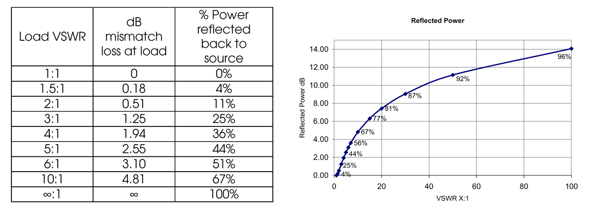
Let’s look at a typical situation where an amplifier with a 50 Ω output is driving a wellmatched antenna with a VSWR of 2:1. It can be seen from the formulas in Annex A that for this VSWR, the load could either be 100 Ω or 25 Ω. From the VSWR equations, 11% of the forward power will be reflected while only 89% will be available for radiation.
To complicate matters, simple devices like cables and connectors contribute to the overall system mismatch since they are not a perfect 50 Ω across the broad frequency range required for susceptibility testing. A short or open, however brief, constitutes an infinite VSWR and 100% of the power is reflected back to the amplifier. It is essential that the RF amplifier be capable of absorbing reflected power from extreme mismatches encountered in normal EMC test applications. The amplifier must not only be capable of providing the necessary power, but it must be rugged and reliable.
Figure 1 demonstrates the exponential rise in reflected power as a function of VSWR. Even a relatively small system VSWR of 2:1 may be cause for concern. Indeed, more typical values ranging from 2:1 to 10:1 result in sufficient reflected power to cause damage to an amplifier that has not been designed to tolerate this amount of reflected power. Amplifiers that are unable to sink large amounts of reflected power must then require protection. One approach is to attach an attenuator at the output of the amplifier. This technique is described in IEC 61000-4-6, where an optional 6 dB pad is inserted between the amplifier and the load. By doing so, the poor load VSWR is improved, and the resulting reflected power is reduced. Not only is there less reflected power, but any reflected power is reduced by 6 dB by the attenuator, further protecting the amplifier. While initially this approach sounds plausible, the downside is that the forward power into the load is also attenuated by 6 dB. (Figure 2) This reduces the power delivered by 4X, thereby requiring an amplifier with 4X the power to compensate.

As mentioned previously, many applications will present poorly matched loads resulting in high reflected power. AR has designed rugged amplifiers that can withstand full reflected power without the need for the IEC protection approach. Hence, no power is lost due to the addition of attenuators.
Class AB amplifiers are typically unable to absorb reflected power. One of the following protection techniques must be used to protect the output stages from reflected power:

The first and second approaches are not desirable since they will shut down the test. Each time an inevitable mismatch occurs not only is the test terminated, there is no apparent means to proceed. Since a “real life” load can not be swapped out with one approaching an ideal 50 Ω, and broadband impedance matching is out of the question, the only practical recourse would be to add a 6-dB attenuator as described above. Unfortunately, as noted previously, this “fix” requires that the amplifier be resized to 4X the original power, which is a hefty penalty to pay.
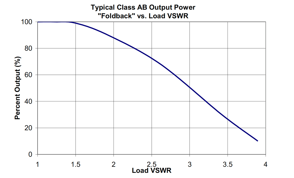
Of the three approaches, the “foldback” scheme is most common. Figure 3 shows a Class AB output power vs. load VSWR curve taken from the manufacturer’s published literature. This curve shows an alarming inability of the RF devices to dissipate even a minimal amount of reflected power. The amplifier must implement a “foldback” of the available RF output power, in an effort to protect its output stages. Specifically, the curve clearly shows that a 100 W amplifier could not sustain even 100 W into a modest typical antenna VSWR of 2.0:1. It reduces its output power to 89 W. Thus, with as little as 11% of the output power reflected, the forward power has dropped to 89 W. Considering a minimal increase in VSWR to a value of 3:1 and with only 25% of the output power reflected back, the Class AB amplifier has cut back its forward power to a meager 50 W. This is clearly not the kind of performance needed in a susceptibility test system which must maintain prescribed field levels, in spite of VSWR variations.
There are situations where the above protection is unable to react quickly enough, or the reflection is of such a magnitude that complete protection is impossible. In these situations, the amplifier is weakened or damaged. An extreme case occurs when a defective cable or load shorts or opens resulting in an infinite VSWR. As a result, 100% of the forward power is reflected back into the output stages of the amplifier. This occurrence is not as rare as one may think. The simple mistake of not thoroughly checking the integrity of all RF cables and connectors before running a test can cause such a catastrophic result.
For EMC susceptibility testing where transducers can typically present high VSWRs, it can be seen that the size, weight, and efficiency advantages of Class AB amplifiers are inconsequential if they are unable to handle reflected power. Just as important to EMC testing is the ability to maintain power over frequency and load. As a result, AB amplifiers are typically not recommended for EMC and high mismatch applications.
In Class A operation, the active devices are biased to ensure that output current flows for 360 degrees of input signal. A properly designed Class A amplifier dissipates maximum power in its quiescent state and must be built to handle a great deal of power dissipation. Contrasted to a Class AB amplifier, the Class A design necessarily requires the use of larger active devices, and quite often, a larger number of devices to share the heat dissipation. Furthermore, additional attention is paid to heat sinking, cooling considerations, and rugged component selection. When rated input signal is applied to an AR designed class A amplifier, the RF devices actually run cooler. Since they are thus operating below their normal operating temperature, power reflections resulting from operating into high levels of VSWR are not a problem, as the devices will still not exceed maximum temperature.
Not all Class A amplifiers are made alike. Some Class A amplifiers are not designed to handle extreme mismatches and may fail instantly or may weaken over time with everyday use. In some cases, Class A amplifiers must institute the same protection features found on a Class AB amplifier. While all Class A amplifiers generally tolerate reflected power better than Class AB amplifiers, some can be damaged by the severe reflected power that occurs when the occasional short or open is encountered while conducting an EMC test. Unfortunately, this is not all that uncommon in busy EMC test facilities, especially when tests are running behind schedule and the pressure is on.
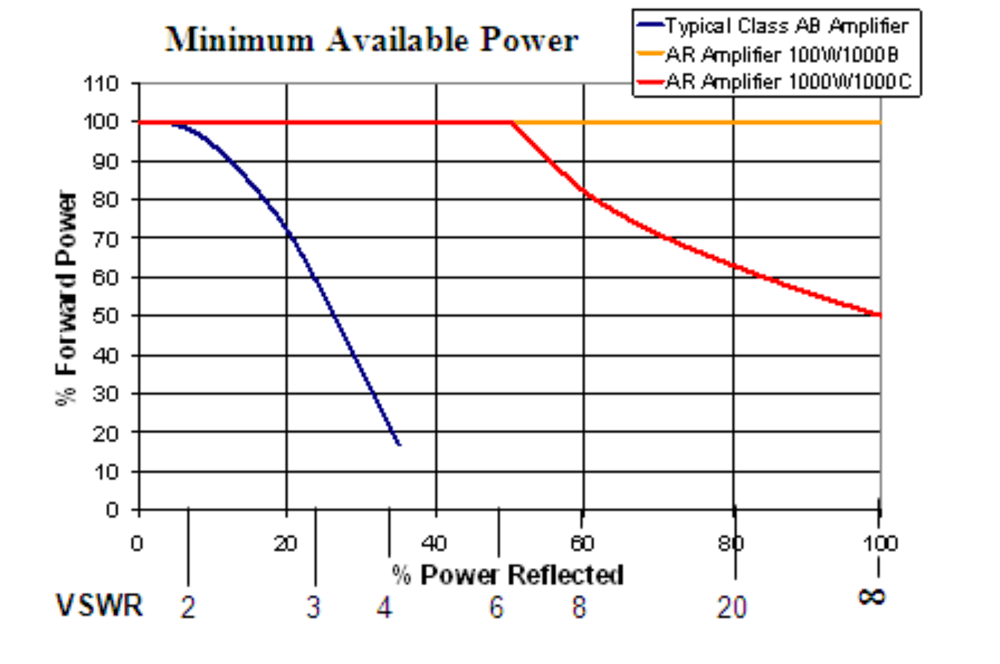
A summary of mismatch performance for typical Class A and AB amplifiers is shown in Figure 3. The 100 W curve is representative of most amplifiers below 500 W. An analysis of our 100W1000B shows that the amplifier delivers a Minimum Available Power (MAP) of 100 W irrespective of the load VSWR, including opens and shorts. As the rated output power of an amplifier increases, it becomes increasingly difficult to absorb all of the reflected power uniformly. Hot spots at these elevated power levels can cause damage or at least affect reliability. Consequently, for rated powers >500 W, AR has developed techniques that continue to offer mismatch tolerance up to a load VSWR of 6:1. Once this level is reached, the output power is limited to 50% of rated power. For example, a 1000 W amplifier will provide a MAP of 1000 W up to a load VSWR of 6:1. At this point approximately 500 W is reflected. From this point on, as load VSWR increases the output power is gradually reduced until it reaches 500 W for an infinite load VSWR. Figure 3 clearly shows the advantage of this implementation when compared to the conventional “foldback” scheme used by typical Class AB amplifiers. In practice, the conservative AR VSWR compromise of 6:1 works well, in that load VSWR is often held to this value or better. If it strays beyond, rest assured your AR amplifier has sensed the increase and has implemented sufficient limiting to protect the amplifier from any damage. See Annex B for a detailed case study of how Class A and Class AB amplifiers deal with mismatch.

AR has taken a ruggedized approach to the design and implementation of our amplifiers. From the very first amplifier developed, to the extensive line of amplifiers offered today, we have understood the extent of mismatch encountered by our customers and are devoted to delivering the maximum output power into any load, regardless of mismatch, without compromising the integrity of the amplifier. A statement of this commitment is found on our data sheets for amplifiers up to 500 W, …”Will operate without damage or oscillation when connected to any load impedance without the aid of foldback circuitry.” For amplifiers > 500 W, the data sheet statement is… “Will operate without damage or oscillation when connected to any load impedance without the aid of foldback circuitry. However, mismatch above 6.0:1 may limit output”.
If you would like to learn more about mismatch tolerance and AR’s approach, feel free to contact one of our applications engineers at 800-933-8181 or visit our website at www.arworld.us.
160 Schoolhouse Rd.
Souderton PA 18964-9990 USA
215.723.8181
[email protected]
[email protected]
Contact Us
For an applications engineer call:
800.933.8181
For Customer Service, call:
215.723.0275
For Faxing Orders:
866.859.0582 (Orders Only, Please)
Privacy Policy
Terms of Use
Copyright ©2023 AR Inc.